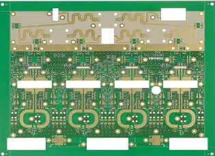
PCB design goal is smaller, faster and lower cost. And because the point of interconnection on the circuit chain is the weakest link, in RF pcb design, electromagnetic properties at the point of interconnection is the main problem faced by the engineering design, to examine each of the points of interconnection and to solve existing problems.
Interconnection of circuit board system comprises three: a chip to a circuit board, interconnects within PCB board and signal input / output interconnect between the PCB and the external device . This paper describes practical skills summary of high frequency PCB design with the nterconnects within PCB board.I believe that by understanding this paper will bring convenience to further PCB design.
In PCB design,chip and PCB interconnect are important for design, but the main problem between chip and pcb interconnect is that too high interconnection density will lead to that the basic structure of PCB material becomes the factor that limit the interconnection density growth.This article shares practical tips of high frequency PCB design.
For high-frequency applications,techniques of interconnect within the high frequency PCB design include:
1, the transmission line use a 45 ° angle to reduce the return loss;
2, Use high-performance insulation board of insulation constant value which are tightly controlled by levels.This approach is conducive to the effective management of electromagnetic field of the insulating material and the near wiring.
3, to perfect specifications of the high-precision etched PCB design,we should consider total error of required line width is +/- 0.0007 inches;that we should manage the undercut and cross section of wiring shape;that we specify plating conditions of the wiring side wall. The wiring geometry and the surface of coating are overall managed,which is very important for solving the skin effect which is related with microwave frequency and for implementing these norms.
4, highlight lead present tapped inductor,which should avoid the use of leaded components.In high frequency environment, it is best to use surface mount components.
5,For the signal vias,it should avoid using the PTH process on the sensitive plate. Because this process can lead to lead inductance on PTH .If a through-hole on a 20-layer board is used to connect the first layer to the third layer,lead inductance can affect 4-19 layers.
6,we should provide a rich ground layer. We can use molded hole to connect the ground layer , to prevent three-dimensional electromagnetic field affect the circuit board.
7. To select the electroless nickel plating or gold plating process, do not use HASL plating method. This can surfacely provide better plating skin effect of high frequency current. In addition, this high weldable coating requires less lead and help reduce environmental pollution.
8, the solder resist layer prevents the solder paste flowing. However, since the uncertainty of the thickness and unpredictability of the insulating properties make the entire surface of the board covered with a solder resist,which will result in large changes of electromagnetic energy in the design of microstrip . Commonly solder dam is used to make the solder resist layer.
The above is for everyone to share high frequency PCB design techniques in the PCB board interconnect.If you are familiar with these methods, we can understand the use of copper backed coplanar microstrip design is more economical and practical than stripline design.