This paper mainly describes four special plating method of the circuit board manufacturing
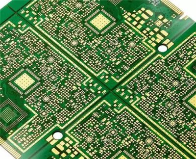
pcb manufacturing
The first kind, refers to the row type electroplating.
It often requires rare metals plated on edge-board connector, edge-board protruding contacts or gold finger,in order to provide low contact resistance and high wear resistance.This technology is called row type plating or projection plating.Often plate gold on the protruding contacts of the edge-board connector whose inner plating layer is nickel. Goldfinger or edge projection use the manual or automatic plating technology.Currently gold on the plug or gold finger has been replaced by rhodium plated, lead plated . The process is as follows:
1) stripping coating and removing tin or tin-lead coating of protruding contacts .
2) Rinse with cleaning water
3) Scrub with an abrasive scrub
4) Activation is immersed in 10% sulfuric acid
5)plate nickel on protruding contacts in the thickness of 4 -5μm
6) Cleaning demineralized water
7) Treatment of gold osmotic solution
8) Gold Plated
9) Cleaning
10) Drying
Second, through-hole plating
There are multiple ways to build a plating layer that can meet the requirement on the hole wall of the drilling hole of the base plate,which is called the activation of walls in industrial applications.PCB manufacturers need a plurality of intermediate slot to produce.Each slot has its own control and conservation requirements.
Through-hole plating is follow-up necessary production process in the process of drilling.When the drill bit drills through the copper foil and the underlying substrate, the heat generated makes insulating synthetic resin which form the majority of substrate melt. The molten resin and other drilling debris accumulate around the hole,and coat on the new exposed hole wall in the copper foil,which is in fact detrimental in the following plating surface. Molten resin will leave heat axis on the hole wall of substrate,which exhibite poor adhesion for most of activator,which requires the development of techniques that is similar to the stain and etch back chemistry.
A method ,which is more suitable product for pcb prototyping, is to use a low-viscosity inks that is specially designed,which is used to form high-adhesive and high-conductive coating film on each through-hole wall.This do not need to use multiple chemical processes ,only one application step, followed by heat curing, which can form continuous coating film in all the inside hole wall .it does not need further processing and can be directly plated.
This ink is a resin-based material.It has a very strong adhesion. It can effortlessly adhere on most polished hole wall,which eliminate the etch-back step.
The third, roll wheel gearing type selective plating
Pins of electronic components, such as connectors, integrated circuits, transistors, and a flexible printed circuit circuit and so on,are all used the selective plating to obtain a good contact resistance and corrosion resistance.This plating method can be used manually, or automatically .The individual selective plating for each pin is very expensive, so you must use mass soldering.
Typically,punch both ends of metal foil whose thickness is required by being flatted.Do the cleaning by chemical or mechanical methods,then selectively use the nickel,gold, silver, rhodium, or tin-nickel alloy, copper-nickel alloy, and nickel lead alloy to continuous plating. In the method of selective plating,firstly,the part which does not need to be plated on the metal copper plate is covered with resist film.Only partly plate in selected copper.
Fourth, brush plating
Another selective plating method is called ” brush plating”.It is an electrode position technique. Not all parts are immersed in an electrolyte during plating.
In this plating technique, only a limited area is plated, but it has no effect on the rest. Typically, make the rare metal plated in selected portions on printed circuit board , such as edge-board connectors .
Brush plating is used more time when maintaining waste printed circuit boards in the electronics assembly workshop. A special anode (chemical reaction is inert , such as graphite) is wrapped in absorbent material (cotton swabs), and use it to bring the plating solution to the required plating place.