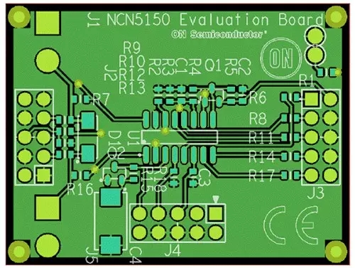
The connection arrangement mode between PCB components.
(1) The printed circuit does not allow to have the cross circuit.For possible cross line,two kinds of solutions :”through” and “around” can be used. That is, let the lead go through from a gap at the foot of the other resistors, capacitors, transistors,or go around from one end of possible cross line.If the circuit is very complicated in exceptional circumstances, in order to simplify the design , jumper wire is allowed, which can solve the problem of cross circuit.
(2) Components,such as resistors, diodes, capacitors and so on,have two installation methods:”vertical” and “horizontal”.Vertical refers to that components are perpendicular to the printed circuit board for the mounting and welding,and its advantage is to save space. Horizontal refers to that components are parallel to and close to the circuit board for mounting and welding.It has the advantage of better mechanical strength of component mounting.These two different installation of components,their element pitch on the printed circuit board is not the same.
(3) A circuit ground point with the same level should be as close as possible.And the power supply filter capacitor of this level should also be on this ground point.In particular, the ground point of base and emitter of this level’s transistor can not be too far away,or the too long copper between the two ground points will cause the interference and the self-excitation.Using this circuit with such “point ground method,”the work is more stable,and it is not easily self-excitation.
(4) Total ground must be in strict arrangement principle with the high frequency – the intermediate frequency – the low frequency .Repetitious random access is not allowed.Wiring would rather be long between levels,we also should comply with this provision.Especially the requirement of the ground wire arrangement of frequency head, playback head, FM head is more stringent. If it is inappropriate,it will produce self-excitation which lead to the failure to work. Frequency circuit ,such as FM lead, often use the large wraparound ground,to ensure good shielding effect
(5) Strong current lead ,such as common ground, amplifier power leads, etc. should be as wide as possible,in order to reduce wiring resistance and voltage,which can reduce the parasitic coupling that may generate the self-excitation.
(6) High impedance traces should be as short as possible. Low impedance traces can be longer, because the high impedance traces are easy to get the line pipe and absorb the signals,which cause the circuit instability.Power lines, ground, base of no feedback element, and emitter lead belong to low-impedance traces. Emitter follower base alignment and the ground of two channels of tape recorders must be separated into their own way until the end of the effect and then together.If two-way ground wire does not separate,it is easy to produce crosstalk and decrease the separation.