Due to the rapid development of high-tech, most electronic products are beginning to use multi-layered pcb. Traditional single and double-sided board can not meet requirements of the design and use. Multilayer PCB fabrication in the whole production has been dominant. For production process of multilayer boards,engineers in R & D job for many years have no chance to go to the pcb factory for understanding the entire production process control.
So, today,I will take the production process of our factory’s order 336058 as an example. From two aspects:the part of engineering design and the part of production process control, I will analysis the production process control of miltilayer pcb for everyone.
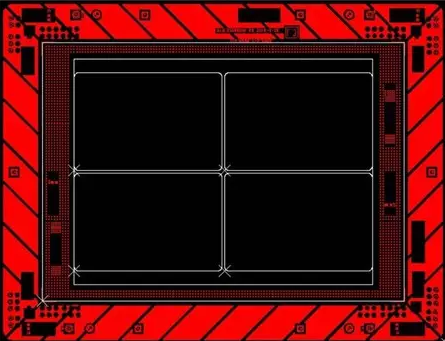
Product Overview – Production Difficulties
Layers is 10,
Minimum mechanical drilling is 0.2mm
L2 ~ L9 is for the buried hole, diameter is 0.2mm
L1 ~ L2 and L9 ~ L10 are for the blind hole, diameter of a blind hole is 0.127mm
Line width and line spacing are both 4mil
The thickness of inner core is 0.2mm,and its copper thickness is H / H oz
Engineering design part
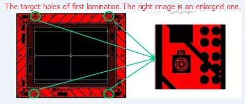
Design of L2 ~ L9
Lamination target hole design of L2 ~ L9
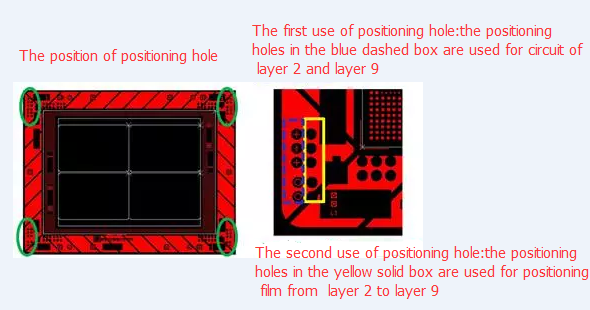
Positioning hole design of L2 ~ L9
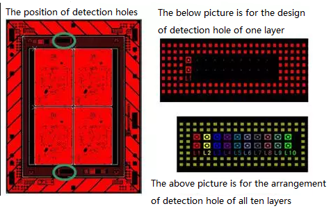
Detection hole design for buried hole of L2 ~ L9
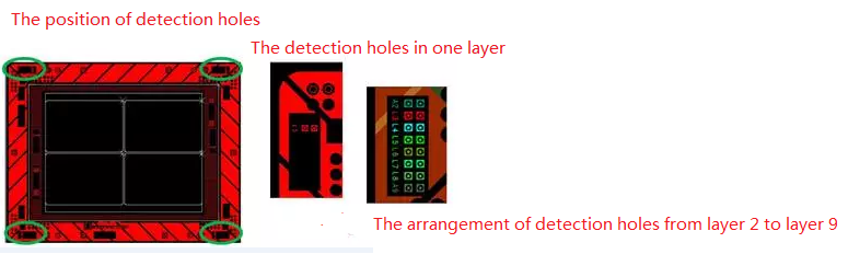
Detection hole use for buried hole of L2 ~ L9
After finishing the lamination from layer 2 to layer 9,before drilliing the buried holes,we must drill the detection hole of buried hole.The size of detection hole and PAD is designed as the size of inner minimum hole.Therefore,when detection hole is detected with a magnifying glass by facing the light,if each layer are located in the PAD,it indicates that drilling the inner buried hole will not break pads.If the detection hole is outside PAD, it indicates that buried hole will deviate from the pad and appear open circuit.

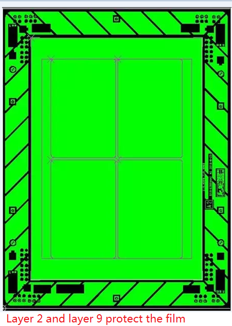
Layer 2 and layer 9 protect film
In the first time of inner layer line, layer 2 and layer 9 are not required to make the line, so when etching the inner layer , these two layers need to be protected with film.
Making line of layer 2 and layer 9
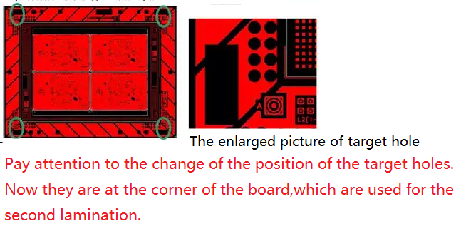
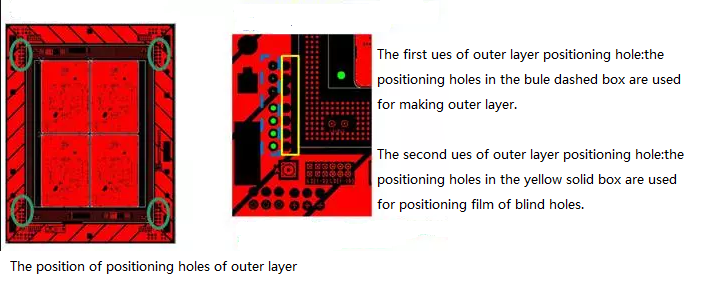
Use the outer positioning hole
Detection hole of drilling hole (1)
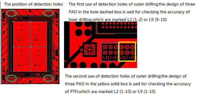
Detection hole of drilling hole (2)
Use the detection hole of drilling hole
The design of these detection hole aims: When drilling, we can firstly drill detecion hole.If the drilled hole are within the range of detection PAD, it shows they are qualified,and the holes can be normally drilled.If the drilled hole are not within the range of detection PAD,it shows harmomegathus betweeen drill belt and board is inconsistent.At this time if the holes in the board are drilled,then mass open circuit will appear.At this time, you need to ask the project to adjust factor of harmomegathus.
NOTE: laser drilling will automatically adjust factor of harmomegathus according to the distance of four target holes.However, it requires that the target hole can not miss and that the bit between inner layers is not offset.
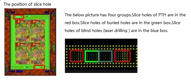
Slice hole
the content of engineering design part has been introduced over,and it is strictly controlled part when cam engineer deal with the production data. The next phase will continue for everyone about the” process control part “.